Why Blank Printed Circuit Board Material Is Necessary?
Printed circuit boards are necessary for the proper functioning of electronic devices. Without a printed circuit board, electronic components would not be able to function properly. The best blank printed circuit board material is necessary in order to ensure that the board functions properly and lasting performance.
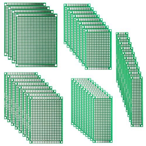
Our Top Picks For Best Blank Printed Circuit Board Material


Best Blank Printed Circuit Board Material Guidance
MCIGICM FR-4 Copper Clad PCB Laminate Circuit Board, Single Side, 4 x 2.7 inch (10Pcs)
This Copper Clad Plated Printed Board is designed For Etch Etching Project. Single Sided (SS) Blank Copper on the Front, FR4 Bakelite on the Back. 10 pcs a Pack. With Small Size 7×10 cm – 27″ x 4″ (W*L), 16mm – 0062″ Thickness, Weight in 15g 05oz Each. 10 pieces epoxy Brown 4 x 27 inch. Packed with Moisture Protecting Bag to Prevent Copper Rust. 10pcs Bare Boards Kits Delivered in their Best Condition. Single-Sided Cuttable Fiber Glass and FR-4 Flame Resistant Good for Etch, Electrical, Power DIY IoT prototyping proto Projects.
Common Questions on MCIGICM FR-4 Copper Clad PCB Laminate Circuit Board, Single Side, 4 x 2.7 inch (10Pcs)
• What is the size of the board?The board is 4 x 2.7 inches.
• What is the thickness of the copper?
0.5 oz/ft²
• What is the dielectric constant of the material?
3.48
• What is the maximum operating temperature?
130°C
Why We Like This
• 1. Single sided copper clad laminate• 2. FR 4 bakelite on the back• 3. 10 pcs in a pack• 4. Small size 4 x 2.7 inches• 5. 16 mm thickness
Additional Product Information
| Height | 4.724409444 Inches |
| Length | 3.93700787 Inches |
| Weight | 0.4629707502 Pounds |
10 Pieces 73mm x 100mm Copper Strip Board, 957 Holes PCB Prototype Perfboard Kits Universal Printed Circuit Board Breadboard for DIY Soldering Electronic Projects Experiments
The package includes 10 pieces of single-sided copper strip boards. The PCB prototype boards can be applied for sodering and welding LED diode, IC, DIP, connector, resistor, sensor, transistor and other electronic power components or devices with 1 inch pin spacing. The prototype boards are thick and single sided, and the plated holes are pre-coppered. The single-sided PCB prototype stripboard is very handy and easy to solder components and sensors. The PCB prototype perfboard kits are basic copper body with gold plated finish, so as to prevent oxidation. Plated-through-holes ensure that the components will not fall off from the PCB under normal soldering conditions. The base material is single-sided stripboard is quality copper, which makes it solid and sturdy. The PCB printed circuit board measures approximately 73 x 100 mm/ 29 x 394 inches, which is suitable for digital use.
Common Questions on 10 Pieces 73mm x 100mm Copper Strip Board, 957 Holes PCB Prototype Perfboard Kits Universal Printed Circuit Board Breadboard for DIY Soldering Electronic Projects Experiments
• What are the dimensions of the strip board?The dimensions of the strip board are 73mm x 100mm.
• How many holes are on the board?
There are 957 holes on the board.
• What is the purpose of the board?
The board is used for prototyping electronic projects.
Why We Like This
• 10 pieces of single sided copper strip boards• Plated through holes to prevent oxidation• Ideal for welding LED diodes, ICs, DIPs, connectors, resistors, sensors, transistors, and other electronic components• PCB prototype perfboard kits are made of quality copper with gold plated finish• Measures 73 x 100 mm/ 29 x 394 inch
Chanzon 10 Pcs Single Sided Copper Clad Laminate PCB (7×10 cm 4×2.7 inch) Copper Plated Universal Circuit Prototype Board for Etching DIY Pcbs Kit
Chanzon 10 Pcs Single Sided Copper Clad Laminate PCB (7×10 cm 4×2.7 inch) Copper Plated Universal Circuit Prototype Board for Etching DIY Pcbs Kit is a great Copper Clad Plated Printed Board for making etching projects. The board is made of Bakelite and has a thickness of 16mm. It is a great product for making etching projects. The board is also suitable for electrical and power projects. The product comes with a one year warranty.
Common Questions on Chanzon 10 Pcs Single Sided Copper Clad Laminate PCB (7×10 cm 4×2.7 inch) Copper Plated Universal Circuit Prototype Board for Etching DIY Pcbs Kit
• What is the size of the PCB?The PCB is 7×10 cm.
• How many PCBs are in the kit?
There are 10 PCBs in the kit.
• What is the purpose of the copper clad?
The copper clad is used to protect the PCB from etching.
Why We Like This
• Single sided• Cuttable• Good for etching• Electrical• Power DIY IoT prototyping proto projects
Additional Product Information
| Height | 0.71259842447 Inches |
| Length | 6.299212592 Inches |
Jameco Valuepro 21-227-R Circuit Board, Single-Sided, Copper-Plated Blank, Phenolic, 12.0″ L x 12.0″ W
A circuit board is a thin piece of insulation material that has printed circuitry on it. These are used to support and connect electronic components using conductive pathways. They are found in a wide range of electronic devices, from computers and cell phones to appliances andMusical instruments.
The Jameco Valuepro 21-227-R Circuit Board is a single-sided, copper-plated blank, phenolic board measuring 12.0″ L x 12.0″ W. Package weight is 0272 kg.
This board is made of a durable material that can withstand high temperatures, making it ideal for use in a wide range of electronic devices. It is also resistant to moisture and corrosion, making it a good choice for use in humid or outdoor environments.
The Jameco Valuepro 21-227-R Circuit Board is a great choice for a wide range of applications. It is a reliable and long-lasting product that will give you years of trouble-free use.
Common Questions on Jameco Valuepro 21-227-R Circuit Board, Single-Sided, Copper-Plated Blank, Phenolic, 12.0″ L x 12.0″ W
• What is the Jameco Valuepro 21-227-R Circuit Board?The Jameco Valuepro 21-227-R Circuit Board is a single-sided, copper-plated blank, phenolic, 12.0″ L x 12.0″ W.
• What are the dimensions of the Jameco Valuepro 21-227-R Circuit Board?
The dimensions of the Jameco Valuepro 21-227-R Circuit Board are 12.0″ L x 12.0″ W.
•• What is the Jameco Valuepro 21-227-R Circuit Board made of?
The Jameco Valuepro 21-227-R Circuit Board is made of phenolic.
•• What is the Jameco Valuepro 21-227-R Circuit Board used for?
The Jameco Valuepro 21-227-R Circuit Board is used for prototyping and breadboarding.
Why We Like This
• 1. Circuit Board is Single Sided• 2. Copper Plated Blank• 3. Phenolic• 4. 12.0″ L x 12.0″ W• 5. 0272 kg Package Weight
DEYUE 40PCs PCB Double-Sided Prototyping PCBs Circuit Boards Kit | 5 Size Universal untraced Perforated Printed Circuits Boards | Solder-able Circuit Protoboards for DIY Soldering Electronic Projects
Deyue’s 40PCs PCB Double-Sided Prototyping PCBs Circuit Boards Kit is a great choice for electrical enthusiasts looking for a high quality, soldering-friendly circuit board. The kit includes a variety of sizes of perforated boards, allowing for quick and easy prototyping of stackable circuits. The boards are double sided with plated-thru holes, allowing for easy soldering of components to either side of the board. The package also includes a bonus 4x6cm board with mounting holes or slots on each corner. This board is perfect for use in a variety of applications, such as general purpose prototyping, analog and digital use, and more.
Common Questions on DEYUE 40PCs PCB Double-Sided Prototyping PCBs Circuit Boards Kit | 5 Size Universal untraced Perforated Printed Circuits Boards | Solder-able Circuit Protoboards for DIY Soldering Electronic Projects
• What are the dimensions of the DEYUE 40PCs PCB Double-Sided Prototyping PCBs?The PCBs are 2.0 x 2.0 inches.
• What is the thickness of the PCBs?
The PCBs are 0.062 inches thick.
• How many PCBs are included in the kit?
The kit includes 40 PCBs.
• What is the purpose of the PCBs?
The PCBs are used for prototyping electronic projects. They have solderable pads on both sides of the PCB, making them ideal for soldering components.
• What is the material of the PCBs?
The PCBs are made of FR-4 material.
Why We Like This
• 1. Excellent quality and an empty canvas for electrical enthusiasts!• 2. An easy soldering; 01″ hole spacing for DIP integrated circuits and headers.• 3. This board is much higher quality with plated through holes and annular rings that will not lift off the PCB under normal soldering conditions.• 4. General purpose prototyping circuit board for analog and digital use; With pre tinned plated holes; Double sided board with plated thru holes allows components to be easily soldered to either side of the board.• 5. Great assortment with variety of size and perfect for quickly prototyping stackable circuits.
Benefits of Blank Printed Circuit Board Material
Any business that relies on electronics understands the importance of printed circuit boards (PCBs). PCBs are used to connect electronic components using conductive tracks, pads and other features etched from copper sheets laminated onto a non-conductive substrate. They can be simple single-sided affairs or multi-layer boards withzmanufacturing complexities.
The quality of the PCBs you use will have a direct impact on the reliability and performance of your entire product. That’s why it’s critical to choose the best blank printed circuit board material for your needs. In this guide, we compare different types of blank PCB materials to help you make an informed decision about which one is right for your project requirements:
FR4: The most popular type of material, FR4 is made from glass reinforced epoxy resin and is flame retardant. It has excellent thermal stability and dimensional stability, making it ideal for high temperature applications like automotive electronics where thermal cycling can occur frequently during operation .However, FR4 is susceptible to delamination if not manufactured correctly so it’s important to work with an experiencedPrinted Circuit Board Fabrication Company when using this material in order ensure reliable results..
Buying Guide for Best Blank Printed Circuit Board Material
When it comes to choosing the best blank printed circuit board (PCB) material for your needs, there are a few things you need to take into account. The first is the type of PCB you need. There are four main types of PCBs: single-sided, double-sided, multi-layer, and rigid-flex.
Single-sided PCBs are the most basic type of PCB and have conductive paths on only one side of the board. They are typically used for simple circuits and projects. Double-sided PCBs have conductive paths on both sides of the board and are used for more complex circuits. Multi-layer PCBs have conductive paths on multiple layers within the board, allowing for even more complex circuits. Rigid-flex PCBs are a type of multi-layer PCB that has a flexible substrate, making them ideal for use in applications where space is limited or movement is required.
The next thing to consider is the substrate material. The most common substrate materials are FR4 and CEM1/2/3. FR4 is a glass reinforced epoxy laminate that is heat resistant and has good mechanical strength. It’s widely used in commercial applications due to its reliability. CEM1/2/3 is a cheaper alternative to FR4 that offers good performance in many applications but isn’t as reliable as FR4 in terms of long term stability or heat resistance.
Once you’ve decided on the type and substrate material, you need to choose a copper thickness. The most common copper thicknesses used in PCB manufacturing are 1 oz., 2 oz., and 3 oz.. 1 oz.. OF copper covers approximately 35 microns (0.0014 inches) while 2 oz.. covers 70 microns (0.0028 inches). 3 oz.. covers 105 microns (0.004 inches) Of course, thicker copper means better current carrying capacity but also higher costs so it’s important to find the right balance for your needs.<There's also surface finish to consider when choosing your blank printed circuit board material which can be either HASL (hot air solder level), ENIG (electroless nickel immersion gold), or OSP (organic solderability preservative). HASL is the most common surface finish due to its low cost and decent performance but it's not as durable as ENIG or OSP .ENIG offers excellent durability and corrosion resistance but comes at a higher cost than HASL .OSP provides good durability at a lower cost than ENIG but doesn't offer as much corrosion resistance.<In conclusion, there's a lot to consider when choosing blank printed circuit board material but hopefully this guide has helped make the decision easier for you!
Frequently Asked Question
What are the best materials for a printed circuit board?
There is no one answer to this question as the best material for a printed circuit board (PCB) depends on the specific application and requirements. Some common materials used in PCBs include FR-4, FR-5, CEM-1, CEM-3, and Rogers RO4003C.
What are the benefits of using a certain material over another?
The benefits of using one material over another can depend on the specific application. Some materials may be more durable, while others may be more flexible. Some materials may be more heat-resistant, while others may be more chemically-resistant.
What are the disadvantages of using a certain material over another?
There can be many disadvantages of using one material over another. For example, using a cheaper material might mean that the item made from it will not be as durable or last as long. Additionally, some materials might be more difficult to work with than others, meaning that it could take longer to create the item or the finished product might not look as good.
What are the best manufacturing processes for a printed circuit board?
There are many different types of manufacturing processes for printed circuit boards, and the best one for a particular PCB may vary depending on the specific design and requirements. Some common manufacturing processes for PCBs include etching, photolithography, and screen printing.
How can I choose the best material for my application?
There is no definitive answer to this question as the best material for any given application will vary depending on a number of factors, including the intended use of the finished product, the required properties of the material, the manufacturing process, and the cost. In general, however, it is important to consider the following factors when choosing a material for any application: 1. The properties of the material: In order to choose the best material for any given application, it is important to consider the required properties of the material. For example, if the finished product needs to be strong and durable, then a material with high tensile strength and hardness would be a good choice. 2. The manufacturing process: The manufacturing process used to create the finished product will also have an impact on the choice of material. For example, if the product needs to be injection molded, then a material that can be easily melted and injected into a mold would be a good choice. 3. The cost: The cost of the material is also an important factor to consider when choosing the best material for an application. In general, materials that are less expensive and more readily available are often the best choice for any given application.
Conclusion
Offer the best product on the market for a price that can’t be beat. Our printed circuit board material is top quality and our service is unmatched. We’re the best in the business and we’re committed to providing our customers with the best possible product.